- 您现在的位置:买卖IC网 > Sheet目录336 > IXDN514SIAT/R (IXYS)IC GATE DRIVER SGL 14A 8-SOIC
�� �
�
�IXDI514� /� IXDN514�
�*� The� following� notes� are� meant� to� define� the� conditions� for� the� θ� J-A� ,� θ� J-C� and� θ� J-S� values:�
�1)� The� θ� J-A� (typ)� is� defined� as� junction� to� ambient.� The� θ� J-A� of� the� standard� single� die� 8-Lead� PDIP� and� 8-Lead� SOIC� are� dominated� by� the�
�resistance� of� the� package,� and� the� IXD_5XX� are� typical.� The� values� for� these� packages� are� natural� convection� values� with� vertical� boards�
�and� the� values� would� be� lower� with� natural� convection.� For� the� 6-Lead� DFN� package,� the� θ� J-A� value� supposes� the� DFN� package� is� soldered�
�on� a� PCB.� The� θ� J-A� (typ)� is� 200� °� C/W� with� no� special� provisions� on� the� PCB,� but� because� the� center� pad� provides� a� low� thermal� resistance�
�to� the� die,� it� is� easy� to� reduce� the� θ� J-A� by� adding� connected� copper� pads� or� traces� on� the� PCB.� These� can� reduce� the� θ� J-A� (typ)� to� 125� °� C/W�
�easily,� and� potentially� even� lower.� The� θ� J-A� for� DFN� on� PCB� without� heatsink� or� thermal� management� will� vary� significantly� with� size,�
�construction,� layout,� materials,� etc.� This� typical� range� tells� the� user� what� he� is� likely� to� get� if� he� does� no� thermal� management.�
�2)� θ� J-C� (max)� is� defined� as� juction� to� case,� where� case� is� the� large� pad� on� the� back� of� the� DFN� package.� The� θ� J-C� values� are� generally� not�
�published� for� the� PDIP� and� SOIC� packages.� The� θ� J-C� for� the� DFN� packages� are� important� to� show� the� low� thermal� resistance� from� junction� to�
�the� die� attach� pad� on� the� back� of� the� DFN,� --� and� a� guardband� has� been� added� to� be� safe.�
�3)� The� θ� J-S� (typ)� is� defined� as� junction� to� heatsink,� where� the� DFN� package� is� soldered� to� a� thermal� substrate� that� is� mounted� on� a� heatsink.�
�The� value� must� be� typical� because� there� are� a� variety� of� thermal� substrates.� This� value� was� calculated� based� on� easily� available� IMS� in� the�
�U.S.� or� Europe,� and� not� a� premium� Japanese� IMS.� A� 4� mil� dialectric� with� a� thermal� conductivity� of� 2.2W/mC� was� assumed.� The� result� was�
�given� as� typical,� and� indicates� what� a� user� would� expect� on� a� typical� IMS� substrate,� and� shows� the� potential� low� thermal� resistance� for� the�
�DFN� package.�
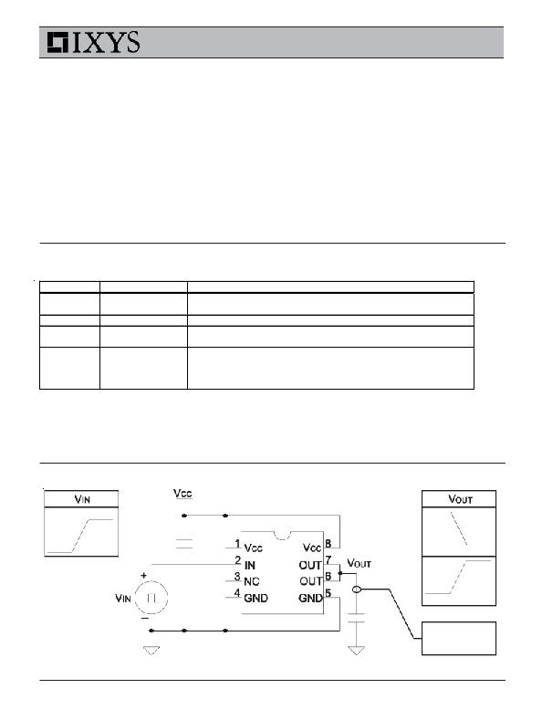
�Pin� Description�
�SYMBOL�
�VCC�
�IN�
�OUT�
�GND�
�FUNCTION�
�Supply� Voltage�
�Input�
�Output�
�Ground�
�DESCRIPTION�
�Positive� power-supply� voltage� input.� This� pin� provides� power� to� the�
�entire� chip.� The� range� for� this� voltage� is� from� 4.5V� to� 30V.�
�Input� signal-TTL� or� CMOS� compatible.�
�Driver� Output.� For� application� purposes,� this� pin� is� connected,�
�through� a� resistor,� to� Gate� of� a� MOSFET/IGBT.�
�The� system� ground� pin.� Internally� connected� to� all� circuitry,� this� pin�
�provides� ground� reference� for� the� entire� chip.� This� pin� should� be�
�connected� to� a� low� noise� analog� ground� plane� for� optimum�
�performance.�
�CAUTION:� Follow� proper� ESD� procedures� when� handling� and� assembling� this� component.�
�Figure� 3� -� Characteristics� Test� Diagram�
�5.0V�
�Vcc�
�15nF�
�0V�
�10uF�
�25V�
�5�
�2500� pf�
�0V�
�IXDI514�
�Vcc�
�0V�
�IXDN514�
�Agilent� 1147A�
�Current� Probe�
�发布紧急采购,3分钟左右您将得到回复。
相关PDF资料
IXDN602PI
MOSFET N-CH 2A DUAL LO SIDE 8-DI
IXDN630CI
IC GATE DRIVER LOW SIDE 5TO220
IXDS430SI
IC DRVR MOSF/IGBT 30A 28-SOIC
IXS839S1T/R
IC MOSFET DRIVER SYNC BUCK 8SOIC
JLINK-RX-AD
ADAPT BD FOR MINI-JTAG CONNECTOR
JMBADGE2008-B
BOARD JM BADGE
JP9902
CONN JACK MOD INSERT W/O HOLES
JTAGJET-C2000
JTAG EMULATOR FOR TI C2000 MCU
相关代理商/技术参数
IXDN514SIATR
制造商:IXYS 制造商全称:IXYS Corporation 功能描述:14 Ampere Low-Side Ultrafast MOSFET Drivers
IXDN55N120
制造商:IXYS 制造商全称:IXYS Corporation 功能描述:High Voltage IGBT with optional Diode
IXDN55N120AU1
制造商:未知厂家 制造商全称:未知厂家 功能描述:TRANSISTOR | IGBT | N-CHAN | 1.2KV V(BR)CES | 85A I(C) | SOT-227B
IXDN55N120D1
功能描述:IGBT 晶体管 55 Amps 1200V RoHS:否 制造商:Fairchild Semiconductor 配置: 集电极—发射极最大电压 VCEO:650 V 集电极—射极饱和电压:2.3 V 栅极/发射极最大电压:20 V 在25 C的连续集电极电流:150 A 栅极—射极漏泄电流:400 nA 功率耗散:187 W 最大工作温度: 封装 / 箱体:TO-247 封装:Tube
IXDN602D2TR
功能描述:IC GATE DVR 2A DUAL HS 8DFN RoHS:是 类别:集成电路 (IC) >> PMIC - MOSFET,电桥驱动器 - 外部开关 系列:- 标准包装:50 系列:- 配置:低端 输入类型:非反相 延迟时间:40ns 电流 - 峰:9A 配置数:1 输出数:1 高端电压 - 最大(自引导启动):- 电源电压:4.5 V ~ 35 V 工作温度:-40°C ~ 125°C 安装类型:表面贴装 封装/外壳:TO-263-6,D²Pak(5 引线+接片),TO-263BA 供应商设备封装:TO-263 包装:管件
IXDN602PI
功能描述:MOSFET N-CH 2A DUAL LO SIDE 8-DI RoHS:是 类别:集成电路 (IC) >> PMIC - MOSFET,电桥驱动器 - 外部开关 系列:- 标准包装:95 系列:- 配置:高端和低端,独立 输入类型:非反相 延迟时间:160ns 电流 - 峰:290mA 配置数:1 输出数:2 高端电压 - 最大(自引导启动):600V 电源电压:10 V ~ 20 V 工作温度:-40°C ~ 125°C 安装类型:表面贴装 封装/外壳:8-SOIC(0.154",3.90mm 宽) 供应商设备封装:8-SOIC 包装:管件 产品目录页面:1381 (CN2011-ZH PDF)
IXDN602SI
功能描述:MOSFET N-CH 2A DUAL LO SIDE 8-SO RoHS:是 类别:集成电路 (IC) >> PMIC - MOSFET,电桥驱动器 - 外部开关 系列:- 标准包装:95 系列:- 配置:半桥 输入类型:PWM 延迟时间:25ns 电流 - 峰:1.6A 配置数:1 输出数:2 高端电压 - 最大(自引导启动):118V 电源电压:9 V ~ 14 V 工作温度:-40°C ~ 125°C 安装类型:表面贴装 封装/外壳:8-SOIC(0.154",3.90mm 宽) 供应商设备封装:8-SOIC 包装:管件 产品目录页面:1282 (CN2011-ZH PDF) 其它名称:*LM5104M*LM5104M/NOPBLM5104M
IXDN602SIA
功能描述:DUAL LOW SIDE MOSFET DRIVER RoHS:是 类别:集成电路 (IC) >> PMIC - MOSFET,电桥驱动器 - 外部开关 系列:- 标准包装:95 系列:- 配置:高端和低端,独立 输入类型:非反相 延迟时间:160ns 电流 - 峰:290mA 配置数:1 输出数:2 高端电压 - 最大(自引导启动):600V 电源电压:10 V ~ 20 V 工作温度:-40°C ~ 125°C 安装类型:表面贴装 封装/外壳:8-SOIC(0.154",3.90mm 宽) 供应商设备封装:8-SOIC 包装:管件 产品目录页面:1381 (CN2011-ZH PDF)